32KB 16K x 16 FLASH AVR 8-Bit Microcontroller AVR® ATmega Series ATMEGA328 28 Pin 20MHz 5V 28-DIP (0.300, 7.62mm)
This article will cover its pinout, datasheet, programming and more detailed information about ATMEGA328-PU.
ATMEGA328-PU Pinout

ATMEGA328-PU Pinout
ATMEGA328-PU CAD Model
Symbol

ATMEGA328-PU Symbol
Footprint

ATMEGA328-PU Footprint
3D Model

ATMEGA328-PU 3D Model
ATMEGA328-PU Overview
The ATMEGA328-PU is a low-power, 8-bit CMOS microcontroller based on the AVR-enhanced RISC architecture. The ATMEGA328-PU achieves throughputs approaching 1MIPS per MHz by executing powerful instructions in a single clock cycle, allowing the system designer to optimize power consumption versus processing speed.
ATMEGA328-PU Features
-
131 powerful instructions, most single clock cycle execution
-
32 x 8 general-purpose working registers
-
Fully static operation
-
Up to 20MIPS throughput at 20MHz
-
On-chip 2-cycle multiplier
-
Write/erase cycles: 10,000 flash/100,000 EEPROM
-
Optional boot code section with independent lock bits
-
In system programming by an on-chip boot program
-
True read while writing operation
-
Programming lock for software security
-
Atmel® QTouch® library support
-
Capacitive touch buttons, sliders and wheels
-
QTouch and QMatrix® acquisition
-
Up to 64 sense channels
-
Two 8bit timer/counters with separate Prescaler and compare mode
-
One 16-bit timer/counter with separate Prescaler, compare mode, and capture mode
-
Real-time counter with separate oscillator
-
Six PWM channels
-
Programmable serial USART
-
Serial peripheral interface (SPI)
ATMEGA328-PU Alternatives
The Alternate Parts for ATMEGA328-PU:
-
ATMEGA328-MUR
-
ATMEGA328-MMHR
-
ATMEGA328-AU
ATMEGA328-PU Block Diagram

ATMEGA328-PU Block Diagram
The AVR core combines a rich instruction set with 32 general-purpose working registers. All 32 registers are directly connected to the Arithmetic Logic Unit (ALU), allowing two independent registers to be accessed in one single instruction executed in one clock cycle. The resulting architecture is more code efficient while achieving throughputs up to ten times faster than conventional CISC microcontrollers.
The ATmega328PU provides the following features: 4K/8Kbytes of In-System Programmable Flash with Read-While-Write capabilities, 256/512/512/1Kbytes EEPROM, 512/1K/1K/2Kbytes SRAM, 23 general purpose I/O lines, 32 general purpose working registers, three flexible Timer/Counters with compare modes, internal and external interrupts, a serial programmable USART, a byte-oriented 2-wire Serial Interface, an SPI serial port, a 6-channel 10-bit ADC (8 channels in TQFP and QFN/MLF packages), a programmable Watchdog Timer with internal Oscillator, and five software selectable power saving modes. The Idle mode stops the CPU while allowing the SRAM, Timer/Counters, USART, 2-wire Serial Interface, SPI port, and interrupt system to continue functioning. The Power-down mode saves the register contents but freezes the Oscillator, disabling all other chip functions until the next interrupt or hardware reset. In Power-save mode, the asynchronous timer continues to run, allowing the user to maintain a timer base while the rest of the device is sleeping. The ADC Noise Reduction mode stops the CPU and all I/O modules except the asynchronous timer and ADC, to minimize switching noise during ADC conversions. In Standby mode, the crystal/resonator Oscillator is running while the rest of the device is sleeping. This allows very fast start-up combined with low power consumption.
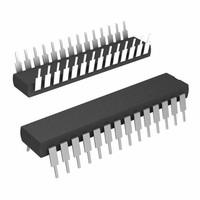
ATMEGA328-PU Package

ATMEGA328-PU Package

- Over 50,000 parts in stock

- One-stop shop

- Original parts at the competitive price

Copyright © 2023 Gobetter Technology CO.,LIMITED
-
E-mail
Yinky@Gobettermall.com -
WhatsApp